

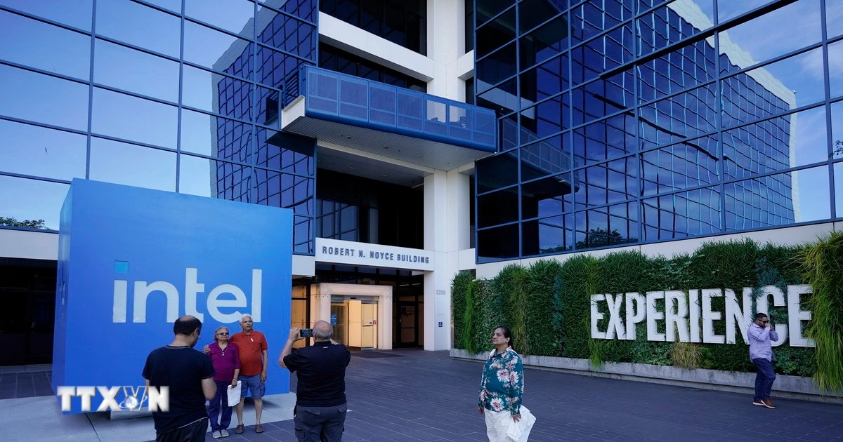
According to PhoneArena , TSMC and Samsung Foundry are expected to start mass producing 2nm chips in 2025, which means that 1.8nm chips will allow Intel to take the lead in chip manufacturing processes. Intel is said to spend between $300 million and $400 million per EUV High-NA machine.

Each ASML High-NA machine costs at least $300 million.
“We are shipping the first High-NA system and announced this in a social media post. The system will be delivered to Intel as planned as previously announced,” ASML said of the delivery.
With a High-NA system, the higher the NA number, the higher the resolution of the pattern etched onto the silicon wafer. While current EUV machines have a .33 aperture (equivalent to 13nm resolution), a High-NA machine has a .55 aperture (equivalent to 8nm resolution). With the higher resolution pattern transferred to the wafer, the foundry may not need to run the wafer through the EUV machine twice to add additional features, saving both time and money.
High-NA EUV machines mainly focus on reducing the size of transistors and increasing the density to pack more transistors inside a chip. The higher the number of transistors on a chip, the more powerful and energy efficient it is. With High-NA machines, transistors can be shrunk 1.7 times with a 2.9 times increase in density.

Each High-NA machine is shipped by ASML in 13 large containers
The new version of the High-NA EUV machine will help make chips 2nm and below. Just last week, TSMC and Samsung Foundry addressed their post-2nm roadmap. The two plan to develop semiconductors using the 1.4nm process by 2027. Production of 2nm chips is expected to begin in 2025, and a few days ago, TSMC allowed Apple to evaluate 2nm chip prototypes.
Transporting the EUV High-NA machine was no easy task as it was divided into 13 large containers and 250 crates. The assembly of the machine was also extremely difficult.
Source link
![[Photo] Prime Minister Pham Minh Chinh chairs the meeting of the Government Party Committee Standing Committee](https://vstatic.vietnam.vn/vietnam/resource/IMAGE/2025/8/23/8e94aa3d26424d1ab1528c3e4bbacc45)
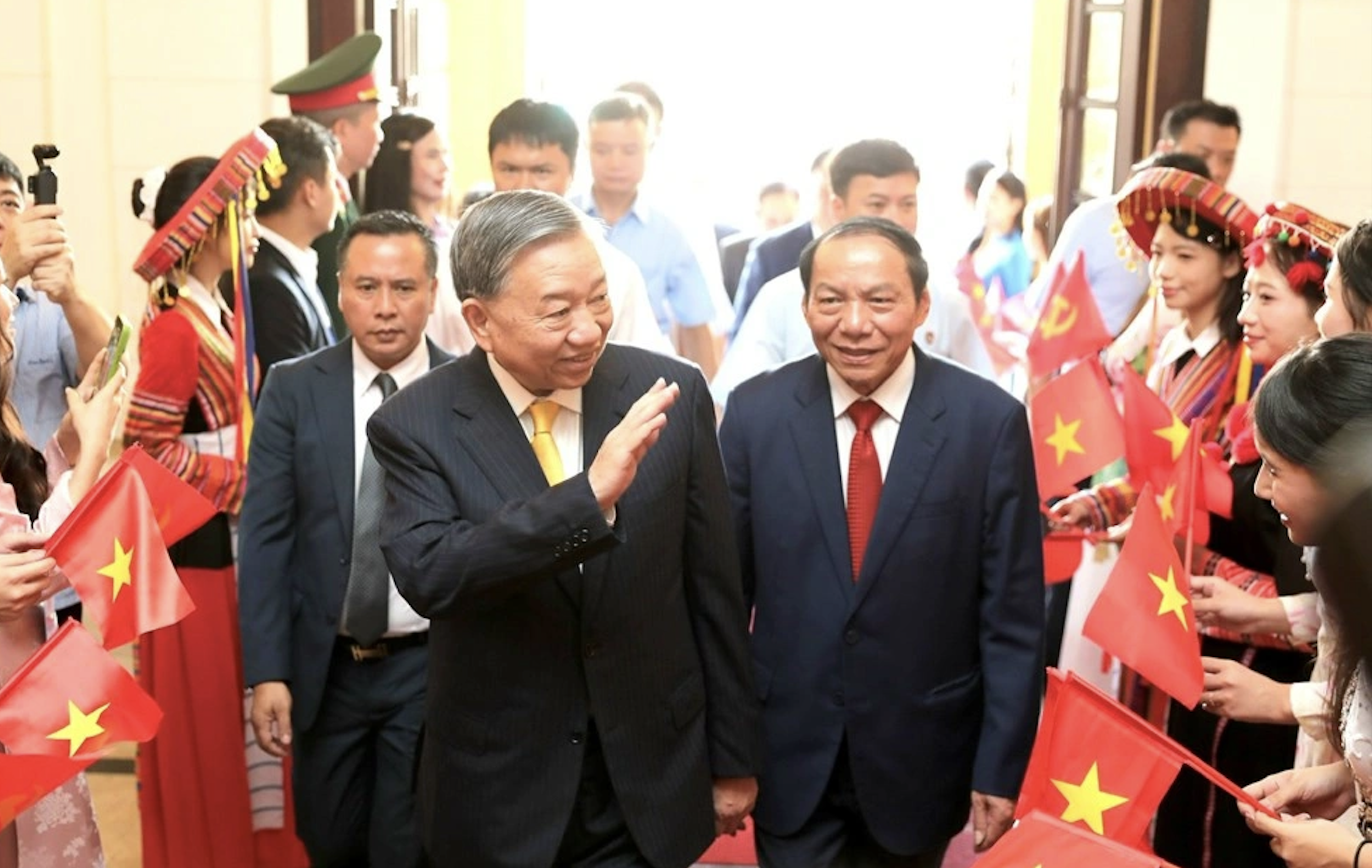
![[Photo] General Secretary To Lam attends the 80th Anniversary of the Cultural Sector's Traditional Day](https://vstatic.vietnam.vn/vietnam/resource/IMAGE/2025/8/23/7a88e6b58502490aa153adf8f0eec2b2)


Comment (0)